





1 Introduction
Microcontrollers are increasingly applied in automated control devices, microprocessor-based integrated protection systems for power grids, and other industrial automation control fields, with the complexity of these devices growing steadily. To address the real-time, multi-tasking demands of development targets, the single-CPU, single-developer model is being replaced by a collaborative approach involving multiple CPUs of various types and multiple developers. This new development paradigm introduces a critical challenge: standardizing the hardware and software for information exchange between CPUs during implementation. This standardization is pivotal to the successful adoption of this new model. Among numerous communication methods, the UART-based RS-485 serial communication protocol is widely adopted due to its simple wiring, high reliability, and ability to support multiple CPUs. Regarding software communication protocols, the Modbus protocol offers significant advantages to users due to its universal nature and mature debugging software. Therefore, during the development of the new motor comprehensive protection device, the RS-485 serial communication method and Modbus communication protocol were adopted to achieve data and control command information exchange between multiple CPUs. To enhance the efficiency and coordination of serial communication, the author implemented numerous measures in the hardware and software architecture of the communication mechanism, achieving excellent results. During the system communication debugging phase, a method was employed where each CPU module first communicated with standard Modbus test software before undergoing mutual interconnection debugging, significantly improving collaborative development efficiency. Practice has proven that this design philosophy simplifies the system structure while greatly enhancing the device's operational efficiency and reliability.
2 Features of the Motor Comprehensive Protection Device
Beyond comprehensive protection functions, the motor protection device integrates measurement, telecontrol, and communication capabilities. Its large-screen Chinese character LCD display enables a user-friendly interface. Utilizing CAN bus communication with the monitoring host, it forms a subsystem within a hierarchical, distributed substation automation system. To optimize system functionality for its multi-tasking requirements, a multi-CPU architecture was adopted. One CPU handles periodic pulse sampling and transmission; the main CPU module manages data processing, electrical parameter calculation, fault diagnosis, and switching operations; while the board module CPU oversees human-machine interaction and facilitates communication with the main protection module and monitoring host. Each CPU module has clearly defined tasks, facilitating collaborative development by multiple engineers during implementation. Serial communication links the main CPU and panel CPU, enabling human-machine interaction and thus occupying a critical position. Establishing a rational communication mechanism is the core of the serial communication section, determining communication coordination and debugging efficiency during the later stages of system development.
3 Introduction to Communication Mechanisms
3.1 Hardware Design of Communication Mechanism
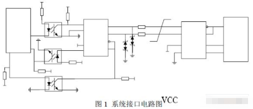
The communication mechanism proposed for this system aims for high efficiency and reliability. RS-485 employs a half-duplex structure, which is often more practical than full-duplex in field applications. Here, a simplified connection using only two signal lines is adopted. The system interface circuit diagram is shown in Figure 1. The TTL logic levels output by the 8051 microcontroller on the main protection module are optically isolated, then converted to RS-495 levels by the MAX485 chip. Subsequently, the MAX485 chip on the panel module converts these back to TTL logic levels for reading by the 8031 microcontroller. On the 8051 microcontroller side, pin P2.7 of parallel I/O port 2 controls the MAX input enable pin RE and output enable pin DE. As shown in Figure 1, when P2.7 outputs a high level, RE is enabled, allowing the microcontroller side to receive data. When P2.7 outputs a low level, DE is enabled, allowing the microcontroller side to transmit data. This approach prevents data loss due to overlapping caused by blind transmission, ensuring high communication quality and reliable transmission speed.
3.2 Communication Protocol
To ensure accurate data transmission between two modules within the protection device, a set of specifications governing information transfer-including transmission modes, data formats, and content-is essential. This constitutes the protocol or communication protocol. Without readily available, mature debugging software, the main CPU module essentially functions as a black box, leading to numerous and difficult-to-overcome challenges during system integration testing. Therefore, the widely adopted Modbus communication protocol was selected and simplified to suit the device's specific requirements, enabling successful inter-module communication with proven effectiveness. Modbus employs a master-slave communication model. The master first sends a communication request command to the slave. The slave then responds to the master with data based on the function code within the request command. Each slave possesses a unique address. Both the request frames sent by the master and the response frames sent by the slave begin with the slave's address. Slaves only read commands addressed to themselves and ignore messages starting with other slave addresses. This functionality is implemented using the 8051 serial port's Mode 2 or Mode 3. This question-and-answer communication model significantly enhances communication accuracy. The RTU transmission mode of Modbus is adopted in this device.
4 Measures to Enhance Communication Reliability
The final two bytes of a Modbus message serve as checksum bytes. RTU communication employs CRC-16 cyclic redundancy check for error detection. Its encoding/decoding mechanism is relatively simple with a low error rate, achievable through computational or programming methods. Several approaches are outlined below:
4.1 Basic Algorithm (Manual Calculation)
Using CRC16-CCITT as an example: the CRC checksum is 16 bits, and the generating polynomial is 17 bits. Suppose the data stream is 4 bytes: BYTE, BYTE, BYTE, BYTE[0];
Shift the data stream left by 16 bits, effectively expanding it by a factor of 256×256. Then perform division by the generator polynomial 0x11021 using non-borrowing division (equivalent to bitwise XOR). The resulting remainder is the CRC checksum. The transmitted data stream consists of 6 bytes: BYTE, BYTE, BYTE, BYTE[0], CRC, CRC[0].
4.2 Computer Algorithm 1 (Bit-Type Algorithm)
1) Place the upper 16 bits (BYTE, BYTE) of the expanded data stream (6 bytes) into a 16-bit register;
2) If the most significant bit of the register is 1, shift the register left by one bit (obtaining the least significant bit from the next byte), then perform an XOR operation with the simplified form of the generator polynomial; otherwise, simply shift the register left by one bit (obtaining the least significant bit from the next byte);
3) Repeat step 2 until the entire data stream (6 bytes) is shifted into the register;
4) The value in the register is the CRC checksum CRC, CRC[0].
4.3 Computer Algorithm 2 (Byte-Type Algorithm) (256^n denotes 256 raised to the power of n)
Represent the byte-ordered data stream as a mathematical polynomial. Let the data stream be BYTE[n] BYTE[n-1] BYTE[n-2] ... BYTE[0] is represented as the mathematical expression
BYTE[n] × 256^n + BYTE[n-1] × 256^(n-1) + ... + BYTE × 256 + BYTE[0], where "+" denotes the XOR operation. Let the generator polynomial be G17 (17-bit), then the CRC code is CRC16.
CRC16 = (BYTE[n] × 256^n + BYTE[n-1] × 256^(n-1) + ... + BYTE × 256 + BYTE[0]) × 256^2 / G17
This involves shifting the data stream left by 16 bits and then dividing by the generator polynomial G17.
Derivation shows that the CRC check code for BYTE[n-1] equals the XOR result of the upper 8 bits of the previous byte's CRC check code Y[n] (YH8[n]) and the current byte BYTE[n-1].
The byte-type algorithm is as follows:
1) Initialize the CRC register group to all "0" (0x0000).
2) Shift the CRC register group 8 bits to the left and store it in the CRC register group.
3) Perform an XOR operation between the original CRC register group's high 8 bits (shifted 8 bits to the right) and the data byte to obtain an index pointing to the value table.
4) Perform an XOR operation between the table value pointed to by the index and the CRC register group.
5) Increment the data pointer. If data processing is not complete, repeat step 2).
6) Obtain the CRC.
5 Measures to Improve Communication Efficiency
5.1 Separate Communication Receive and Transmit Tasks
The 8051 microcontroller can transmit and receive data via the serial port using interrupts. The serial port controller SCON supports initialization and bit addressing. When a serial port interrupt request occurs, the lower two bits of SCON latch the transmit and receive interrupts. When the CPU writes data or a character to the serial port's transmit buffer SUBF (instruction: MOV SUBF, A) the transmitter begins sending. After completing one data frame, the hardware sets the TI flag to "1", indicating the serial port is requesting an interrupt from the CPU to send the next data frame. Similarly, if the serial port receiver is enabled for reception, upon receiving a frame of data, the RI flag is set to 1, indicating that the serial port is requesting an interrupt from the CPU to read data from the receive data buffer.
5.2 Reducing Interrupt Duration
Since multiple interrupts are employed in the software architecture design, to ensure reliable program operation and minimize the probability of conflicts between different tasks, the software implementation should strive to streamline the tasks of various interrupts and shorten their execution time. Within the communication interrupt subroutine, perform essential tasks upon entering the interrupt, such as: clearing the corresponding status bits in the serial port control register, reading received characters or writing characters to be transmitted from/to the buffer, incrementing the count of received or transmitted characters, etc. Then exit the interrupt immediately. Other tasks, such as validating frames, responding to received frame commands (telemetry/telecommand), and preparing transmission frames, should be handled within the main program.
5.3 Efficient Frame Termination Detection to Prevent Communication Stagnation
Utilizing a dedicated software timer to detect the end of a received frame prevents communication tasks from lingering if a frame is received incompletely, thereby ensuring timely reception of subsequent frames. Since the time interval between bytes within a frame is much shorter than the frame-to-frame interval, the software timer is started each time a new byte is received. The timer is set to the minimum frame-to-frame interval. This interval varies with different baud rates. If the next byte is received before the preset time elapses, it indicates the frame is incomplete, and the timer restarts. If the timer successfully counts down to the preset time, it triggers the corresponding interrupt number. Within the timer interrupt subroutine, the frame end flag byte is set, signifying the frame reception is complete. After the master program detects a frame reception completion, it validates the frame's integrity by verifying the slave address and cyclic redundancy check (CRC) byte. If confirmed as a valid frame intended for the master, it processes the frame command based on its function code and prepares to send a frame. When the slave receives an incorrect message, it sends back an error frame. If the received message has an incorrect CRC, the slave may choose not to respond. If the master does not receive a response from the slave within the specified time, it will retransmit the request message. If multiple retransmissions fail to receive a response from the slave, a communication failure is reported.
5.4 Determining Communication Speed
Since all devices reside within the same chassis, the distance between modules is minimal. Modbus operates on RS485 for long-distance communication, eliminating the need to consider distance effects on baud rate. Furthermore, the master-slave communication mode prevents line congestion. Therefore, from the perspective of communication efficiency, as long as the set baud rate does not exceed the maximum baud rate limit of the chip used in the module, a higher baud rate results in faster information exchange and higher communication efficiency. Setting the baud rate to be exactly the same for both communication parties ensures that the receiving end samples each data bit at the midpoint of the bit cycle, thereby achieving reliable communication.
5.5 Reasonable Debugging Methods
During debugging, first test communication between each CPU module and the microcomputer via the RS485/RS232 data conversion module. After successful individual testing, proceed to inter-module debugging, significantly improving overall debugging efficiency. During module-to-computer communication debugging, the computer employs Modbus debugging software to simulate the master's communication process, actively requesting information from the slave. This makes the entire reception and transmission process transparent and clear, enabling timely resolution of module issues. During joint debugging, bus monitoring software observes data from both sides to promptly identify and resolve problems.
6 Innovation Points of This Paper
First, this paper adopts Modbus, a universal industrial standard, in the protection device. The required tool software can be directly obtained from relevant websites without incurring intellectual property costs. Second, the protection device implements multitasking and utilizes the Modbus protocol to create a reasonable joint debugging mechanism between CPU modules, greatly improving the efficiency of collaborative system development.