




Industrial control systems continue to rely on standard analog signals to transmit data between process and control equipment. Stable 4 to 20mA current loop signals can easily traverse thousands of feet, while ±5 and ±10V signals are also commonplace in industrial systems.
This application note showcases Maxim's integrated data acquisition system (DAS) solutions. Maxim's DAS solutions save board space, power consumption, and design time while converting standard industrial analog signals with minimal external components.
Introduction
Despite multiple versions of digital fieldbuses, industrial control systems continue to rely on standard analog signals to transmit data between process and control equipment. For example, process transmitters in chemical plants convert low-level temperature and pressure signals into stable 4 to 20mA current loop signals that can easily travel thousands of feet.
Speed and position sensors for machine tools and automated guided vehicles in factory automation environments generate unipolar and bipolar voltage signals, typically ranging from 0V to 5V, 0V to 10V, ±5V, or ±10V. Additionally, signals from commonly used PT100 temperature sensing elements often require no conversion and can be directly utilized within standard ranges, such as 10V or 20mA. As RTDs (Resistance Temperature Detectors) made from platinum (Pt), PT100s exhibit a resistance of 0Ω at 100°C. Their resistance exhibits a linear relationship with temperature and provides a relatively high output signal level (>1mV when driven by a 100mA current source).
Control functions within the process environment are implemented by PLCs (Programmable Logic Controllers), PCSs (Process Control Systems), or (more recently) IPCs (Industrial Personal Computers). Since these devices are digital systems running process-specific software, all analog signals must be converted to digital before the computer can read them.
A/D conversion within control systems is performed by boards or boxes termed "analog peripherals." These connect to the CPU via the system's backplane bus or fieldbus when remotely installed (e.g., on machinery). Beyond digital circuitry (for CPU communication), these peripherals incorporate various precision analog and mixed-signal components. The need for more channels per board or smaller packages (for machine mounting) leads to space and power constraints, presenting the primary design challenge for analog peripherals. The following circuit illustrates signal conditioning techniques and describes a method for digitizing up to eight channels using a single chip.
Data Acquisition System
The advanced data acquisition system (Figure 1) comprises a multiplexer (mux) for switching between input channels, a signal conditioning circuit providing gain and offset adjustment for different input ranges, and an analog-to-digital converter (ADC) with a reference voltage (VREF).
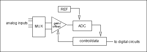 Figure 1. This diagram illustrates the basic components of the data acquisition system.
Integrated DAS Solutions
By integrating the basic modules shown in Figure 1, Maxim has developed a series of single-chip data acquisition systems that save board space, power consumption, and design time. These chips require minimal external components (none in some cases) and can convert most standard signals currently in use. Each device incorporates a 12-bit ADC, multiplexer, and gain/offset correction, featuring a serial or parallel digital interface for easy connection to most microprocessors.
The following block diagram (Figure 2) illustrates a typical configuration for this series. The primary differences lie in the digital section connected to the microprocessor. Each chip provides 16 or 5 single-ended analog input channels connected to the internal ADC via fault-protected multiplexers. Any channel can withstand input voltages up to <>.<>V, and a fault on any channel does not affect conversions on any other channel.
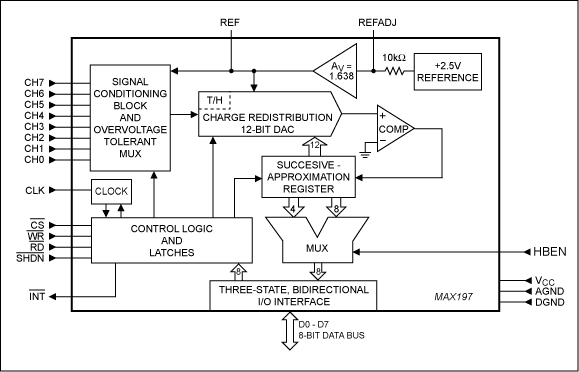 Figure 2. The functions shown in Figure 1 are integrated into this chip.
Each channel can be independently programmed for a standard input range (0 to 5V, 0 to 10V, ±5V, or ±10V) while being powered by a single 5V supply. Other devices feature similar gain structures but accept different input ranges: unipolar or bipolar 2V or 4V, or unipolar or bipolar VREF or -VREF. The 100x gain variation capability with 10% input offset (from -10V to +2V) expands the dynamic range by 14 bits, resulting in systems with <>-bit dynamic range.
The internal ADC is a 12-bit successive approximation type based on a capacitive DAC, where the MSB capacitance also functions as the hold capacitor in the sample/hold circuit. Each device can operate using either the internal oscillator or an external clock.
The MAX196 to MAX199 devices utilize /WR pulses to start and stop acquisition, providing relatively long acquisition times in "external acquisition mode" without slowing conversion speed. The device's short aperture delay and low aperture jitter (<50ps in external clock/acquire mode) enable precise control of acquisition timing. This capability is critical for phase-sensitive applications such as power line control and AC motor control. Additionally, the chip's wideband input architecture provides up to 5MHz small-signal bandwidth, allowing undersampling techniques beyond the Nyquist frequency.
Digital Interface
Applications requiring high-speed measurements are best served by parallel data interfaces (MAX196 to MAX199). These devices achieve 2Ksps throughput at 100MHz clock rates, sufficient for most high-speed control loops. For lower-speed applications, available I²C-compatible interface versions save board space and simplify communication between DAS and microcontrollers. These devices feature fast conversion times (10μs), but the serial interface limits their throughput to 8kbps.
For example, the MAX197 accepts 0V to 10V, 0V to 5V, ±5V, and ±10V inputs. The source impedance driving these inputs is a primary concern for users. During sampling, the ADC draws a current pulse to charge its T/H capacitor (the MSB capacitor for capacitive DACs). Therefore, a fast-settling operational amplifier with sufficient slew rate is required to ensure adequate voltage settling during acquisition. The MXL1013/MXL1014 operational amplifiers perform well in achieving fast sampling rates. For slower operational amplifiers, the acquisition time must be extended.
Differential inputs used in many automation systems are relatively insensitive to common-mode interference. In most cases, a simple differential amplifier circuit (Figure 3) with input impedance exceeding 1MΩ suffices. (For higher input impedance, use a standard 3-op-amp instrumentation amplifier.) The output shown in Figure 3 is
Vout = R2(V+ - V-) / R1.
For high common-mode rejection, set R1 = R3 and R2 = R4. The gain of the shown combination is 0.876, extending the ±10V input range by approximately 114% to measure signals beyond the range. This adjustment reduces the resolution of the ±10V band to approximately 11.8 bits.
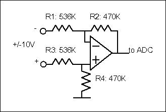 Figure 3. A simple differential amplifier provides high input impedance and single-ended output.
20mA Current Loop
Current loops transmit small signals over long distances in noisy environments. The current is typically generated by a process transmitter, which converts variables such as temperature or pressure into a direct current within the 0mA to 20mA or 4mA to 20mA range. The current then flows through a shunt resistor, creating a proportional voltage drop that is easily digitized. Since the compliant voltage available to drive the loop-including wire resistance-rarely exceeds 15V to 18V, the resistor value is limited to a few hundred ohms (Figure 4).
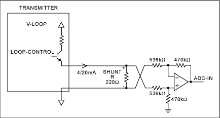 Figure 4. Combining the amplifier shown in Figure 3 with the current loop signal derived from the 220Ω shunt resistor produces a convenient single-ended output.
This circuit features the same differential amplifier as the ±10V conditioning circuit, along with a 220Ω shunt resistor. This resistor exhibits a voltage drop of 4.20V at 4mA and 5.25V at 5mA. The differential amplifier's gain is adjusted at the ADC input to a maximum of 4.62V. Therefore, a DAS programmed for a 0.5V input can digitize this signal with a maximum resolution of 11.8 bits.
Because the MAX198/MAX199 and MAX128 have the smallest input range in this series, they operate with a small shunt resistor without requiring gain adjustment. This makes them more suitable for 10mA measurements in systems that do not require other high-level measurements (up to ±20V). To adapt the circuit shown in Figure 4 for use with the MAX199, configure the MAX199 for a 0 to 2V input range and change the 536kΩ resistor to 470kΩ. Use an 86Ω shunt resistor.
Sensor Adaptation
Thermocouples, strain gauges, and other common sensors provide low-level nonlinear signals that are sensitive to EMI. Therefore, before sending this information to the control system, a 4-20mA transmitter first linearizes and conditions the signal. For less critical temperature measurement applications, resistance temperature detectors (RTDs) can measure temperatures up to 850°C over long distances without requiring expensive signal conditioning.
The most popular RTD is the standardized platinum temperature sensor known as the PT100, featuring a resistance of 0Ω at 100°C and a linear temperature coefficient of 0.38Ω/°C. It also exhibits a smaller nonlinear temperature coefficient, making its Ω/°C characteristic nearly linear over a narrow range. Unlike thermocouples, where the voltage output represents the temperature difference between two points, the RTD's resistance directly represents the absolute temperature of the sensor.
Measurement is achieved by driving a 1mA to 2mA current through the sensor and measuring the voltage drop across its terminals. Higher currents introduce measurement errors due to self-heating caused by increased power dissipation within the sensor. An internal 4.096V reference simplifies the generation of the sensor excitation current (Figure 5).
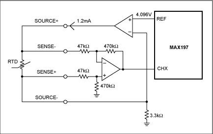 Figure 5. This circuit supplies current to the RTD sensor and digitizes the resulting output.
To prevent wire resistance from affecting measurement accuracy, four independent wires connect the RTD to the differential amplifier. Since the sensing wires connect to the amplifier's high-impedance input, their current is very low, resulting in negligible voltage drop. The 4096mV reference voltage and 3.3kΩ feedback resistor set the excitation current to approximately 4096mV/3.3kΩ = 1.24mA. Consequently, driving both the ADC and current source with the same reference voltage enables a ratio measurement where reference voltage drift does not affect the conversion result.
Configure the MAX197 for a 0V to 5V input range and set the differential amplifier gain to 10 to measure resistance values up to 400Ω, representing approximately 800°C. The microprocessor can linearize the sensor signal using a lookup table. To calibrate the system, replace the RTD with two precision resistors (100Ω representing zero, 300Ω or higher representing full scale) and store the conversion results.
Rather than dedicating specific circuits to particular input ranges, the circuit shown in Figure 6 adapts the ADC input to accommodate any signal range described earlier. Selecting the input pin and ADC input range (Table 1) allows choosing the appropriate configuration.
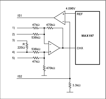 Figure 6. This universal input circuit adapts the ADC to the signal range on each input channel.