




Circuit timing is a critical function required by many electronic devices, including microcontrollers, USB, Ethernet, Wi-Fi, and Bluetooth interfaces, as well as computing devices and peripherals, medical devices, test and measurement equipment, industrial control and automation, the Internet of Things (IoT), wearable devices, and consumer electronics. While designing a crystal-controlled oscillator to provide system timing may initially seem straightforward, designers must consider numerous parameters and design requirements when matching the quartz crystal with the oscillator IC.
There are several factors to consider, including crystal motion impedance, resonance mode, drive power, and oscillator negative resistance. In terms of circuit layout, designers must account for PCB parasitic capacitance, add a protective band around the crystal, and incorporate on-chip capacitors. The final design must be compact and reliable, with the fewest components, low root mean square (RMS) jitter, and minimal power consumption across a wide input voltage range.
A simple packaged crystal oscillator (SPXO) is one solution. These continuous voltage oscillators are optimized for low power consumption and low RMS jitter and can operate at any voltage between 1.60 V and 3.60 V, enabling designers to achieve a solution that can be integrated into the system with minimal design effort.
This article will briefly discuss some of the important performance requirements that must be met and design challenges that must be overcome when designing timing circuits using discrete quartz crystals and timing ICs. It will then introduce Abracon's SPXO solutions and explain how designers can use these devices to effectively meet the timing requirements of electronic systems.
Crystal Oscillator Operation and Design Challenges
Power consumption is a critical consideration for small battery-powered wireless devices. Many such devices are based on ultra-low-power system-on-chip (SoC) radios and processors that can support battery life spanning several years. Additionally, since the battery is often the most expensive component in the system, minimizing its size is crucial for controlling device costs. That said, standby current is often the most critical battery life consideration in small wireless systems, and standby current is often dominated by the clock oscillator. Therefore, it is crucial to minimize the current consumption of the oscillator.
Unfortunately, designing a low-power oscillator can be challenging. One method of saving energy is to minimize standby current by entering a "disabled" state and starting the oscillator when needed. However, requiring a crystal oscillator to start quickly and reliably is no easy task. Designers must ensure that the oscillator remains in a low-current state during standby and has reliable startup characteristics under all operating and environmental conditions.
The Pierce oscillator configuration is commonly found in low-power wireless SoCs (Figure 1). The Pierce oscillator is constructed using a crystal (X) and load capacitors (C1 and C2), surrounded by an inverting amplifier with an internal feedback resistor. Under suitable conditions, when the amplifier's output is fed back to the input, a negative resistance is generated, leading to oscillation.
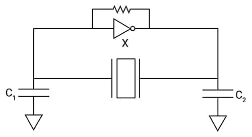 Figure 1: Basic Pierce oscillator configuration built around crystal (X) and load capacitors C1 and C2.
The crystal structure is complex; this discussion only covers the top layer and simplified structure of crystals operating in oscillators.
Closed-loop gain margin Gm can be used as a figure of merit (FOM) to describe the reliability of an oscillator relative to various losses. Closed-loop gain margin is also referred to as oscillation margin (OA). An OA value below 5 can lead to low production throughput and temperature-related startup issues. Designs with an OA value of 20 or higher are robust and durable, operate reliably within the design operating temperature range, and exhibit minimal impact from different production batches on crystal and SoC performance characteristics.
To measure the oscillator's OA, a variable resistor Ra can be added to the circuit (Figure 2). Increase the Ra value until the oscillator fails to start. This is the method used to determine the OA value, as shown below:
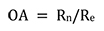
Equation 1
Where:
Rn is the negative resistance
Re is the equivalent series resistance (ESR).

Equation 2

Equation 3
Where the load capacitance CL is calculated as follows:

Equation 4
where Cs is the variable capacitor of the circuit, with a capacitance value typically between 3.0 and 5.0 pF.
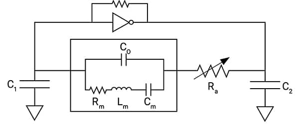 Figure 2: Shows the extended crystal model (middle box) and the adjustable resistor (Ra) used to measure the oscillation margin.
OA depends on ESR (Re), and ESR depends on the quartz crystal parameters Rm and load capacitance CL. For low-power oscillators, such as those used in low-power wireless devices, the influence of Rm and CL on OA increases. Measuring OA is time-consuming and may prolong the development process. Therefore, this task may be neglected, leading to performance issues when the system or device is put into production.
Additionally, setting a high OA to ensure reliable oscillator operation can cause other issues. For example, while a higher OA improves oscillator circuit performance, it may overlook power losses caused by the crystal. Such losses can be a significant factor. Referring to Figure 2, the crystal's motion resistance Rm causes power dissipation as current flows periodically through the resistor. When CL is large, it increases both current and losses. Therefore, designers need to balance crystal power loss with a reasonable OA value.
Avoiding jitter
When designing a quartz crystal oscillator, it is important to understand and reduce jitter. Jitter has two types, typically measured by the root mean square (RMS) value:
Period jitter: Also known as phase jitter, this refers to the maximum time difference between several measured oscillation periods, typically measured over at least 10 periods.
Cycle jitter: This is the maximum variation in a clock edge, measured for each cycle rather than multiple cycles.
The primary sources of jitter in quartz crystal oscillators include power supply noise, integer harmonics of the signal frequency, improper loading and termination conditions, amplifier noise, and certain circuit configurations. Depending on the source, different methods can be employed to minimize jitter.
Use bypass capacitors, chip inductors, or resistor-capacitor (RC) filters to control power supply noise.
In critical applications requiring extremely low jitter, establishing a method to control harmonics is crucial (beyond the scope of this article).
Reduce the power reflected back to the output by optimizing load and termination conditions.
Avoid designs that include phase-locked loops, multipliers, or programmable functions, as they often increase jitter.
Continuous Voltage Crystal Oscillators
Using Abracon's ASADV, ASDDV, and ASEDV SPXOs is advantageous for designing systems where the bias voltage varies between 1.60 and 3.60 V (Figure 3). The SPXO series covers different frequency ranges; ASADV devices operate at frequencies from 1.25 MHz to 100 MHz, while the ASDDV and ASEDV devices operate from 1 MHz to 160 MHz. The series complies with RoHS/RoHS II standards and uses sealed ceramic surface-mount device (SMD) packaging. Within the operating temperature range of -40°C to +85°C, the series achieves frequency stability of ±25 ppm.
OA depends on ESR (Re), and ESR depends on the quartz crystal parameters Rm and load capacitance CL. For low-power oscillators, such as those used in low-power wireless devices, the influence of Rm and CL on OA increases. Measuring OA is time-consuming and may prolong the development process. Therefore, this task may be neglected, leading to performance issues when the system or device is put into production.
Additionally, setting a high OA to ensure reliable oscillator operation can cause other issues. For example, while a higher OA improves oscillator circuit performance, it may overlook power losses caused by the crystal. Such losses can be a significant factor. Referring to Figure 2, the crystal's motion resistance Rm causes power dissipation as current flows periodically through the resistor. When CL is large, it increases both current and losses. Therefore, designers need to balance crystal power loss with a reasonable OA value.
Avoiding jitter
When designing a quartz crystal oscillator, it is important to understand and reduce jitter. Jitter has two types, typically measured by the root mean square (RMS) value:
Period jitter: Also known as phase jitter, this refers to the maximum time difference between several measured oscillation periods, typically measured over at least 10 periods.
Cycle jitter: This is the maximum variation in a clock edge, measured for each cycle rather than multiple cycles.
The primary sources of jitter in quartz crystal oscillators include power supply noise, integer harmonics of the signal frequency, improper loading and termination conditions, amplifier noise, and certain circuit configurations. Depending on the source, different methods can be employed to minimize jitter.
Use bypass capacitors, chip inductors, or resistor-capacitor (RC) filters to control power supply noise.
In critical applications requiring extremely low jitter, establishing a method to control harmonics is crucial (beyond the scope of this article).
Reduce the power reflected back to the output by optimizing load and termination conditions.
Avoid designs that include phase-locked loops, multipliers, or programmable functions, as they often increase jitter.
Summary
Designers require accurate and reliable oscillators to provide stable timing across a wide range of applications and operating temperatures. Discrete crystal-controlled oscillators can meet the required performance characteristics, but it is technically challenging to design effectively using crystals, which is time-consuming and results in unnecessary costs. Additionally, they are not the optimal choice in terms of form factor.
As shown in the figure, designers can utilize low-power integrated SPXOs. These SPXOs form a ready-to-use timing solution, achieving excellent frequency stability across a very wide operating temperature range. By using SPXOs, designers can reduce the number of components, minimize solution size, lower assembly costs, and enhance reliability.